

What Is A Shift Register? Digital Logic
Definition: A shift register is a sequential logic excursion that acts every bit a unit to store and transfer binary data. Basically shift registers are bidirectional FIFO circuit, that shifts every single scrap of the information present in its input towards its output on each clock pulse.
We know registers are the circuits constructed using flip-flops for storing binary data. Ane-bit of information is stored past each flip-bomb at a fourth dimension. So, the storage of multiple bits of data requires multiple flip-flops.
Thus the storing capacity of the register depends on the number of flip-flops used in its structure.
Shift registers are formed by the series combination of D flip-flops, where each flip-flop in the arrangement holds unmarried data chip. The serial arrangement permits the output of ane flip-flop to act as input to other and this allows the shifting of data bit inside the register.
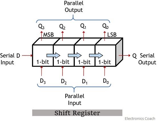
Information technology is to exist noted here that data tin be transferred in or out of the annals either serially or parallely. So, the data flake motion inside the shift register requite rise to various configurations which are as follows:
- SISO: Series-in Serial-out: It permits the insertion of data serially and taking the output likewise in a serial way.
- SIPO: Serial-in Parallel-out: Here the data is inserted serially either from the left or right direction. Just the output is taken parallely.
- PISO: Parallel-in Serial-out: This type of shift register allows the parallel input of data fleck, only the output is taken serially.
- PIPO: Parallel-in Parallel-out: PIPO shift register permits both in and out of data bit in a parallel manner.
Operation of SISO Shift Register
As we have already discussed that a SISO is a type of shift register in which the input is fed serially and output is also taken in serial manner.
Then consider a connection of 4 D flip-flops D0 to Dthree every bit shown in the figure beneath:
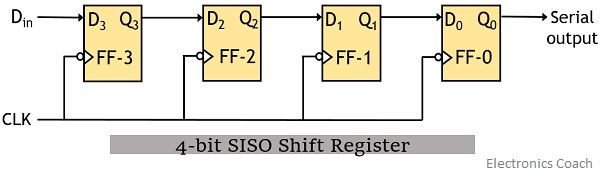
Initially, we consider all the flip-flops are at reset manner. Thus the output of each flip-bomb in the arrangement is logic depression i.e., 0.
Here we have assumed a shift right mode circuit as the information input is nowadays at the left end while the stored scrap is getting shifted towards the right so every bit to provide serial output.
Allow us now sympathise how information is stored in a shift annals.
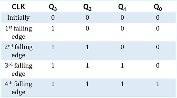
Suppose we take to insert '1111' inside the shift annals. Initially, as the device is in reset manner thus the output of each annals will be low, thereby providing output of all the iv registers as 0000.
- Now beginning with LSB of the data to exist inserted so 1 is provided as input to the circuit i.e., D3 = one. But every bit initially the output of all the flip-flops were 0. Therefore, D2, D1 and D0 will be 0. While input D3 = 1 volition cause Q3 to be 1. Thus the overall output volition be 1000.
- Farther, when another information input bit i.e., 1 is provided at D3. Then over again this will cause Q3 to be 1, but as Qthree is provided every bit input to Dii. Therefore, this volition cause Qii to be 1, while residual all other outputs will be 0. Thus for a second falling edge, we will get 11 at the stored bit inside the register, thereby giving the overall output as 1100.
- Similarly, when iiird input bit 'one' is provided and so previous output Q2 volition cause the input D1 to be 1. This will provide output Q3, Q2 and Q1 every bit i while Q0 will nonetheless remain 0. Thus the overall output will be 1110.
- Furthermore, when MSB of the data is provided as input, then i at Q1 will cause D0 input to be logic loftier. Then, this will cause Q0 to exist 1.
Thus in this fashion shift annals stores '1111' thereby showing in the output.
The figure below represents the truth table for the 4-chip SISO shift annals:
Considering the in a higher place table let us take a look at the waveform representation of a SISO shift register:

Here the first figure shows the clock input bespeak while the 2d figure shows the data input to be stored which is 1111 for this detail case. Thus nosotros take shown continuous high betoken in case of data input.
Also, the above figure represents the 4 data output of the flip-flops.
Initially, all the outputs were 0, this is conspicuously shown in the waveform representation. Notwithstanding, the output Qiii changes from 0 to ane on arrival of starting time clock pulse. While residuum other outputs are still 0.
In a similar way, the 2d clock pulse changes Qtwo from 0 to 1. Thus now both Q3 and Q2 are showing logic high in the waveform representation.
Then, in this way the above figure is clearly showing the SISO operation of the shift register and on the inflow of 4th clock pulse the output of all the 4 registers volition be 1. Equally the storage is performed by shifting each fleck on the arrival of each clock pulse thus it is named so.
Applications of Shift Registers
The different configurations of shift registers provide uses in various fields like a SISO shift annals is used to generate time delay in digital circuits. A SIPO shift register can human action every bit serial to parallel converter.
In a similar fashion, PISO shift register changes parallel input into serial output thereby performing the task of a parallel to series converter.

What Is A Shift Register? Digital Logic,
Source: https://electronicscoach.com/shift-register.html
Posted by: fosterrismustriog.blogspot.com
0 Response to "What Is A Shift Register? Digital Logic"
Post a Comment